As semiconductor processes advance to 3nm, 2nm and beyond, environmental test chambers become critical for full-chain reliability verification, spanning wafer fabrication, packaging, testing and end-use. They simulate extreme conditions to expose latent defects, underpinning high-quality industry development.
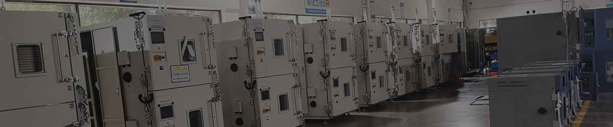
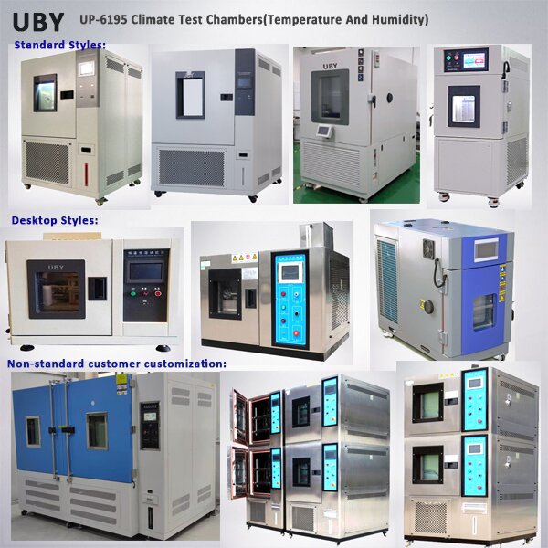
Basic Temperature & Humidity Chambers
Indispensable for R&D and production, they deliver core environmental validation:
- High-low temperature chambers (-65°C to 175°C, ±0.5°C fluctuation) verify wafer stability and solder joint resistance, complying with AEC-Q100 Grade 0.
- Temperature-humidity cycling chambers perform 85°C/85%RH dual 85 testing (IEC 60068-2-78) to detect package delamination and pin oxidation.
- Constant temp-humidity chambers (±2%RH accuracy) support wafer fabrication and burn-in, meeting ISO 17025 standards.
High-End Specialized Chambers Tailored for aerospace and automotive electronics:
- Thermal shock chambers (-55°C to 125°C, 20°C/min transition) reveal hidden defects (JESD22-A104, MIL-STD-810H).
- HAST and triple-combination chambers accelerate aging and integrate temp-humidity-vibration simulation.
- Salt spray, low-pressure and UV aging chambers test corrosion resistance, high-altitude stability and weatherability.
Today’s chambers evolve toward ±0.1°C precision and smart IoT connectivity, supporting advanced devices like Chiplets. As “quality gatekeepers”, they drive the industry to break bottlenecks and capture high-end markets.
Post time: Jan-22-2026